| "ЖУРНАЛ РАДИОЭЛЕКТРОНИКИ" N 9, 2000 |
PLANE WAVE DIFFRACTION BY TWO-DIMENSIONAL GRATINGS OF INDUCTIVE AND CAPACITIVE COUPLING ELEMENTS
Yu. N. Kazantsev, V. P. Mal’tsev, E.S. Sokolovskaya, A. D. Shatrov
Institute of Radioengineering and Electronics, Russian Academy of Sciences
Received September 27, 2000
Frequency selective structures (FSS) in the form of two-dimensional gratings with non-resonant elements are investigated. It is shown that selective properties of these band reflective FSSs are realized at the rejection frequency when the inductive and capacitive terms in the transmission coefficient are cancelled mutually. Expressions for the reflection and transmission coefficients for the gratings consisting of thin metal rectangles are obtained. Also a set of similar FSSs with inductive and capacitive coupling elements is considered. The results of calculations are compared with experimental data.
1. Introduction
Usually frequency selective structures (FSS) are applied for frequency separation in dual frequency band antennas and for back scattering decreasing in radomes.
It is well known that gratings with conductive resonant elements of different shapes represent band-reflective FSSs [1-7]. At the resonant frequency, each element of the grating strongly scatters an incident wave, and therefore the grating reflects the wave completely. So, at the resonant frequency, the reflection coefficient is close to unity, and the transmission coefficient is close to zero.
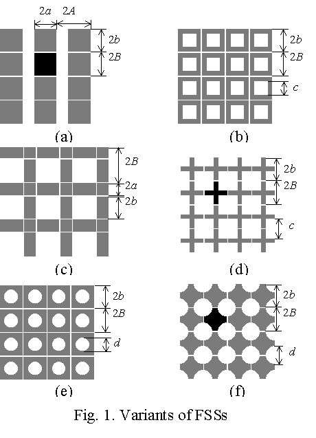
Here we propose another method for the design and investigation of the band-reflective FSSs, when the grating is formed of both inductive and capacitive coupling elements in a conductive screen. For example, non-resonant round or square holes as well as sufficiently wide slots parallel to electric field serve as the inductive coupling elements. Narrow slots perpendicular to electric field represent the capacitive coupling elements. Note that the holes in the well-known pass-band FSSs [8-13] are resonant. Fig.1 shows some variants of investigated FSSs. Dark segments correspond to conductive parts and white segments correspond to slots and holes. The FSS shown in Fig.1a represents the array of mutually orthogonal narrow and wide slots cut in the thin conductive screen (or, which is the same, the two-dimensional array of metal rectangles). The FSS shown in Fig.1b represents an array of square holes and mutually orthogonal narrow slots cut in the thin conductive screen. The structures shown in Figs.1c and 1d are nearly the same as is in Fig1b, except the arrangement and the number of slots. In turn, the structures presented in Figs.1e and 1f differ from the structures 1b and 1d, respectively by the shape of the holes (round instead of square). The structure shown in Fig.1a operates at one incident wave polarisation when the electric field is parallel to the wide slots. The remaining structures can operate at two orthogonal polarisations.
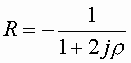
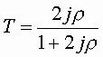
The operation principles of these FSSs can be explained in the following way. The reflection and transmission coefficients for the structures under consideration may be written as
where ρ is the so-called transparency [14]. Transparency ρ can be approximately expressed as
The term ![]() is due to the inductive coupling elements. It is positive and proportional to
frequency. The term
is due to the inductive coupling elements. It is positive and proportional to
frequency. The term ![]() is due to the capacitive coupling elements. It is negative and inversely
proportional to frequency. At certain frequency
is due to the capacitive coupling elements. It is negative and inversely
proportional to frequency. At certain frequency ![]() (rejection frequency), the terms
(rejection frequency), the terms ![]() and
and ![]() are
cancelled mutually and the transmission coefficient vanishes, whereas the
reflection coefficient tends to unity.
are
cancelled mutually and the transmission coefficient vanishes, whereas the
reflection coefficient tends to unity.
Note that some of the structures shown in Fig.1 do not differ from well-known resonance ones in their geometry.
The structures in Figs.1a, 1b and 1d may be considered as
two-dimensional gratings with flat dipoles [3], square loops [7]
and crossed dipoles [4] respectively. (A single grating element
in Figs.1a, 1b and 1d is drawn in black.) The structures in Figs.1b and 1c may
be considered as inverse gridded square or round elements arrays. The
characteristic of the FSSs under consideration is the fact that the elements are
located closely to each other and resonate collectively at frequency ![]() .
The size of the elements may be substantially less than the rejection wavelength
.
The size of the elements may be substantially less than the rejection wavelength
![]() . It ensures
the absence of the grating side lobes in the reflected field.
. It ensures
the absence of the grating side lobes in the reflected field.
Note, all considered structures are total transmitting at the high frequency band due to eigen resonances of inductive coupling elements.
Previously the problem of scattering by a two-dimensional
grating represented in Fig.1a was solved by numerical methods [3].
We obtain the approximate analytical solution when the grating periods do not
exceed the wavelength and the grating elements are extended along the E-vector
of the incident field. The inductive ![]() and capacitive
and capacitive ![]() terms of the transparency r are obtained in explicit
form in the case of small (in comparison with l )
grating periods. We also give the expressions for evaluating the reflection and
transmission coefficients of the FSSs shown in Figs.1b and 1e. We investigate
experimentally all the variants of FSSs presented in Fig.1.
terms of the transparency r are obtained in explicit
form in the case of small (in comparison with l )
grating periods. We also give the expressions for evaluating the reflection and
transmission coefficients of the FSSs shown in Figs.1b and 1e. We investigate
experimentally all the variants of FSSs presented in Fig.1.
2. Two-dimensional grating with thin metal rectangles
Problem formulation
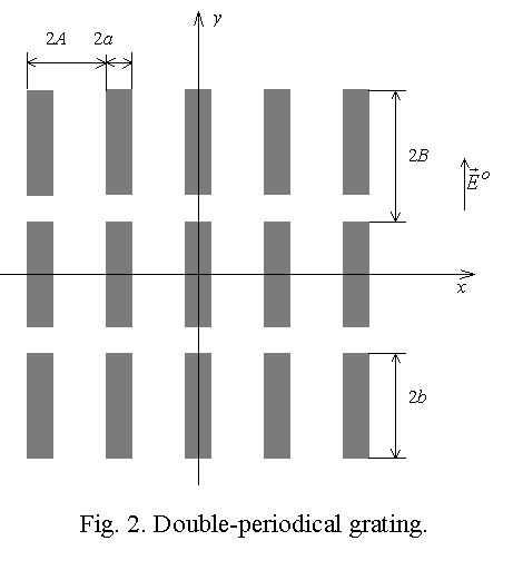
Let a plane wave
be normally incident upon the two-dimensional grating with thin metal rectangles. The grating periods along the x and y-axes are 2A and 2B respectively; the rectangle dimensions are 2a and 2b (Fig.2). We assume at first, that the grating parameters satisfy the conditions
Due to the periodicity of the structure, it is sufficient to
consider a problem within a single period of the structure ![]()
![]() . The incident field induces a
surface current through the metal rectangle
. The incident field induces a
surface current through the metal rectangle ![]()
![]() , which creates the scattered
field
, which creates the scattered
field ![]() . In view of
. In view of ![]() we can neglect the x component of the current [3] and,
consequently, x component of the electric field. In this approximation
the electric Hertzian potential
we can neglect the x component of the current [3] and,
consequently, x component of the electric field. In this approximation
the electric Hertzian potential ![]() has only one component
has only one component ![]() which satisfies the equation
which satisfies the equation
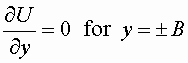
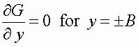
and the Neumann conditions at the boundaries
![]()
![]()
The function ![]() represents the y component of surface current, which is nonzero only
inside the metal rectangle
represents the y component of surface current, which is nonzero only
inside the metal rectangle ![]()
![]()
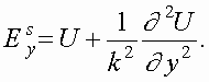
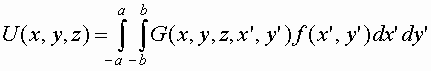
The electrical vector of the scattered field is expressed in
terms of ![]() by the formula:
by the formula:
Its y component is given by
The tangential component of the total electric field satisfies the zero boundary condition on the metal surface:
Integro-differential equation for the current
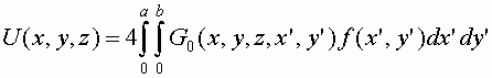
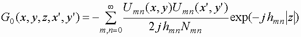
Let us introduce the Green's function ![]() of the rectangular waveguide
of the rectangular waveguide ![]() as
a solution of the equation
as
a solution of the equation
subject to the Neumann boundary conditions on the walls
In addition the function ![]() is assumed to satisfy the waveguide radiation condition; i.e. this function must
not contain any waves incoming from infinity.
is assumed to satisfy the waveguide radiation condition; i.e. this function must
not contain any waves incoming from infinity.
The functions ![]() ,
,
![]() , and
, and ![]() are related by the well-known formula [15]
are related by the well-known formula [15]
Since ![]() is an even function of both co-ordinates, this formula can be rewritten as
is an even function of both co-ordinates, this formula can be rewritten as
where ![]() is the even part of the function G.
is the even part of the function G.
The function ![]() can be represented as an expansion in terms of the waveguide eigen-functions:
can be represented as an expansion in terms of the waveguide eigen-functions:
where
Under conditions (5), the propagation constants of higher modes are imaginary, and we can use the approximation
Therefore, the reflection coefficient is determined by the
single expansion term ![]() of
expression (15) and is given by
of
expression (15) and is given by
The relation
Taking into account (14), we obtain from (22) the integro-differential equation for the current f(x, y):
where
The solution of the equation (23) is sought for the class of functions satisfying the following condition for the current on the rectangle edge [15]
Reduction of the problem to a real equation
The kernel of equation (23) is complex: ![]() .
The imaginary part of the function L is determined by the single
expansion term
.
The imaginary part of the function L is determined by the single
expansion term ![]() of expression (15), which is constant:
of expression (15), which is constant:
In this case, the complex solution ![]() of equation (23) is proportional to the function
of equation (23) is proportional to the function ![]() ,
which is the solution of the real equation
,
which is the solution of the real equation
It follows from (23), (26), (27) that
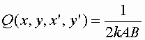
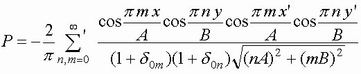
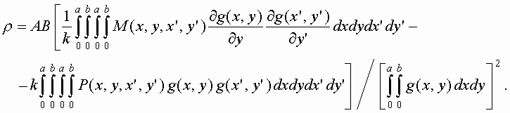
Using expression (1) for the reflection coefficient, we obtain from (21) and (28) that the grating transparency r is expressed in terms of the function g(x, y) as follows
Taking into account (24), (15)-(19), the kernel of integro-differential equation (27) can be represented as
Here the symbol ![]() denotes that the term m=0 and n=0 is omitted in the sum.
denotes that the term m=0 and n=0 is omitted in the sum.
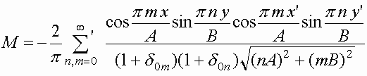
Functions ![]() ,
satisfying condition (25) also satisfy the relation
,
satisfying condition (25) also satisfy the relation
where
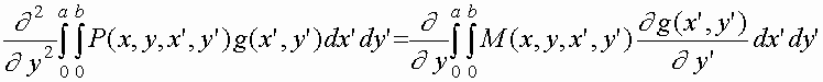
This relation is obtained in a usual way by changing the order of differentiation and integration (see, for example, [15]).
Taking into account (31), we rewrite equation
(27) in the
form  . (33)
Variational method
The kernels ![]() and
and ![]() of
equation (33) are invariant under the permutation
of
equation (33) are invariant under the permutation ![]() .
Using this property we obtain the stationary representation
.
Using this property we obtain the stationary representation
When the condition ![]() is valid, it is appropriate to take a test function in the stationary
functional (34) in the form of the product
is valid, it is appropriate to take a test function in the stationary
functional (34) in the form of the product
where ![]() and
and ![]() are the functions of the surface current distribution in two particular cases,
respectively:
are the functions of the surface current distribution in two particular cases,
respectively: ![]() (the grating with metal strips, which are parallel to electric field
(the grating with metal strips, which are parallel to electric field ![]() )
and
)
and ![]() (the
grating with metal strips perpendicular to electric field
(the
grating with metal strips perpendicular to electric field ![]() ).
We use the known analytical solution of the plane wave diffraction problem on a
small-period grating with metal strips [14]:
).
We use the known analytical solution of the plane wave diffraction problem on a
small-period grating with metal strips [14]:
where ![]() and
and ![]() . The
function
. The
function ![]() has a singularity of the type
has a singularity of the type ![]() at the strip edges. The function
at the strip edges. The function ![]() tends to zero as
tends to zero as ![]() at the strip edges; therefore, function (35) satisfies condition
(25).
at the strip edges; therefore, function (35) satisfies condition
(25).
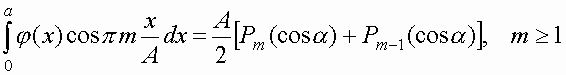
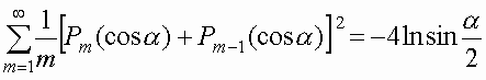
Substitute the expressions (35) - (37) into the stationary representation (34). To calculate the integrals and the sums, we use the formulae
where ![]() are the Legendre polynomials.
are the Legendre polynomials.
As a result, we obtain the expression.
When ![]() or
or ![]() , this
expression turns into the expression for the transparency r
of a metal strip grating in the case of E or H-polarisation,
respectively [14].
, this
expression turns into the expression for the transparency r
of a metal strip grating in the case of E or H-polarisation,
respectively [14].
The transparency (46) contains the inductive and capacitive
terms. At a certain frequency ![]() ,
when these terms are cancelled (i. e.
,
when these terms are cancelled (i. e. ![]() ),
the total reflection effect is observed.
),
the total reflection effect is observed.
This theory did not take into account the effect of
dielectric substrate with permittivity e on which the
metal rectangles are placed in a real grating. We can take into account this
effect approximately by introducing the correction factor ![]() into the capacitive terms of expression (46):
into the capacitive terms of expression (46):
This correction factor is advisable when dielectric substrate
is present only on one side of the grating, the substrate thickness s is
small in comparison with the wavelength in dielectric ![]() and large as compared to the narrow slots width
and large as compared to the narrow slots width ![]() .
.
In the derivation of expression (46), we take into account
that the propagation constant (17) of the mode ![]() is real while the other modes are imaginary. For this to be true, it is
sufficient that the grating parameters satisfy the conditions
is real while the other modes are imaginary. For this to be true, it is
sufficient that the grating parameters satisfy the conditions
instead (5). These conditions ensure the absence of grating side lobes in the scattered field. In this case, we cannot neglect the dependence on k of the kernels of the integro-differential equation (33):
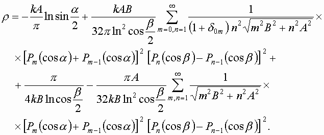
Therefore the inductive and capacitive terms cannot be expressed in explicit form like in the expressions (46), (47). Instead of (47) we obtain the following series expansion for the transparency in terms of the Legendre polynomials:
It is supposed that ![]() Here, we have taken into account the correction factor
Here, we have taken into account the correction factor ![]() .
.
Comparison of calculation results with experimental data
For the experimental verification of the theory, we prepared
seven specimens of the grating shown in Fig.1a. These and all other specimens
described below are made from a 12 m m thick
aluminium foil deposited on 100 m m thick mylar (![]() )
substrate. The basic dimensions and the rejection frequencies of the specimens
are given in Table 1.
)
substrate. The basic dimensions and the rejection frequencies of the specimens
are given in Table 1.
|
Specimen No. |
2a, cm |
2b, cm |
2A, cm |
2B, cm |
Rejection frequency,
|
|
|
Measured |
Calculated |
|||||
|
1 |
0.10 |
0.498 |
2 |
0.50 |
11.67 |
11.57 |
|
2 |
0.23 |
0.498 |
2 |
0.50 |
9.69 |
10.17 |
|
3 |
0.40 |
0.498 |
2 |
0.50 |
9.69 |
9.7 |
|
4 |
0.62 |
0.498 |
2 |
0.50 |
9.39 |
9.75 |
|
5 |
0.70 |
0.498 |
2 |
0.50 |
9.69 |
9.90 |
|
6 |
1.00 |
0.498 |
2 |
0.50 |
9.92 |
11.00 |
|
7 |
1.20 |
0.498 |
2 |
0.50 |
10.80 |
12.30 |
The theory considered here takes into account only the y component of the surface currents through the grating rectangles. It may be inadequate when the longitudinal and transverse dimensions of the rectangle are commensurable. The experimental measurements enabled to estimate the applicability of the theory as these dimensions approach to each other.
The transmission and reflection coefficients were calculated with the formulae (1) and (2), where the transparency ρ was computed from (51).
We will represent the experimental and calculated data by solid and dashed curves, respectively.
Figs.3-5 show the experimental and calculated results for
specimens No 1, 3, 6 (see Table 1). The comparison of the experimental data with
the theory shows that they are in a good agreement for specimens 1-5, i.e. up to
values of ![]() .
.
Figs.6-8 display the calculated frequency dependences of the transmission and reflection coefficients for different parameters of the grating.
The rejection frequency band and the rejection frequency essentially depend on the grating period 2A (Fig.6). When the period 2A decreases and other parameters are constant, the rejection frequency band increases, and the rejection frequency also increases. The grating dimensions are indicated in the figure caption.
When the grating period 2A and the rectangle width 2a are changed simultaneously so that the width of the inductive coupling slots is constant, the rejection frequency is changed weakly, while the rejection frequency band is changed considerably (Fig.7).
When the grating period 2B and the rectangle length 2b are changed simultaneously so that the width of the capacitive coupling slots is constant, the rejection frequency band is changed weakly, while the rejection frequency is displaced considerably (Fig.8).
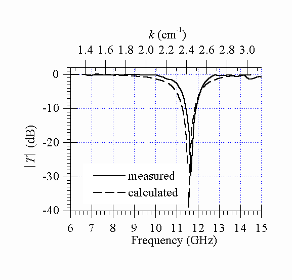
Fig.3. Transmission coefficient for specimen No 1 versus frequency.
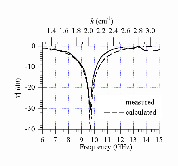
Fig.4. Transmission coefficient for specimen No 3 versus frequency.
Fig.5. Transmission coefficient for specimen No 6 versus frequency.
Fig.6. Calculated transmission and reflection coefficients for structure 1a,
2A is variable, 2a = 0.2 cm, 2B = 1.2cm, 2b = 1.198 cm.
Fig.7. Calculated transmission and reflection coefficients for structure 1a,
2A and 2a are variable, 2b = 1.198 cm, 2B
= 1.2cm, ![]() cm.
cm.

Fig.8. Calculated transmission and reflection coefficients for structure 1a,
2B and 2b are variable, 2a = 0.2 cm, 2A
= 1.2cm, ![]() cm.
cm.
3. Other gratings
For investigating the frequency dependences of the transmission and reflection coefficients for all structures shown in Fig.1, we prepared six more specimens. Their basic dimensions are given in Table 2.
|
Specimen No. |
2B, cm |
2b, cm |
2A, cm |
2a, cm |
c, cm |
d, cm |
Rejection frequency |
|
|
Measured |
Calculated |
|||||||
|
8, Fig.1a |
1.20 |
1.198 |
1.20 |
0.2 |
– |
– |
8.25 |
7.39 |
|
9, Fig.1b |
1.20 |
1.198 |
– |
– |
0.90 |
– |
4.4 |
4.40 |
|
10, Fig.1c |
1.20 |
1.198 |
– |
0.50 |
– |
– |
10.3 |
– |
|
11, Fig.1d |
1.20 |
1.198 |
– |
– |
0.90 |
– |
9.0 |
– |
|
12, Fig.1e |
1.20 |
1.198 |
– |
– |
– |
0.90 |
5.1 |
4.49 |
|
13, Fig.1f |
1.20 |
1.198 |
– |
– |
– |
0.90 |
11.3 |
– |
The results of measurements and theoretical estimations of these dependences are represented in Figs.9-14.

Fig.9. Transmission and reflection coefficients for specimen No 8 versus frequency.
Fig.10. Transmission and reflection coefficients for specimen No 9 versus frequency.
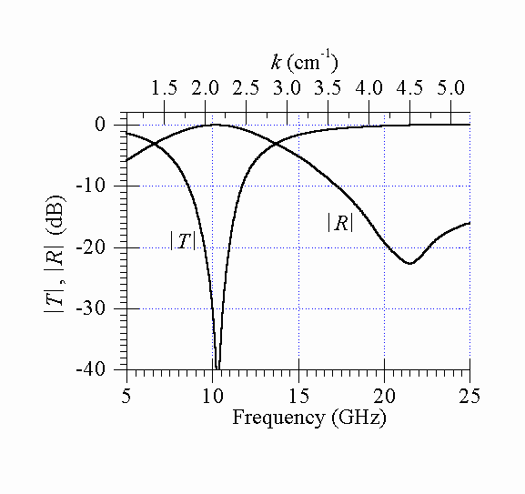
Fig.11. Measured transmission and reflection coefficients for specimen No 10 versus frequency.
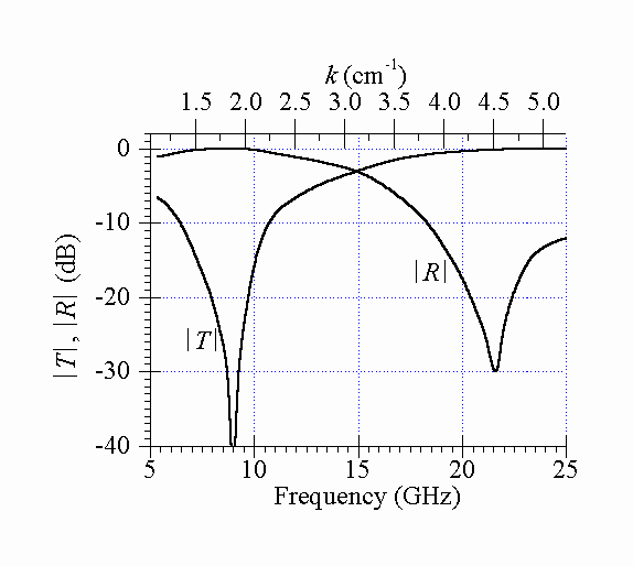
Fig.12. Measured transmission and reflection coefficients for specimen No 11 versus frequency.
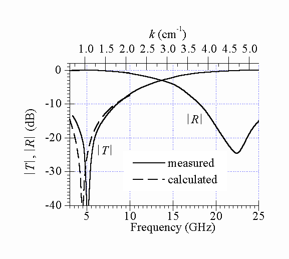
Fig.13. Transmission and reflection coefficients for specimen No 12 versus frequency.
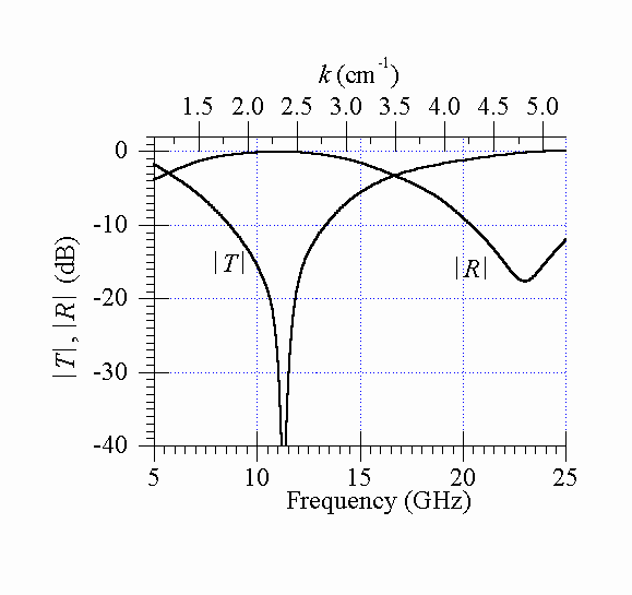
Fig.14. Measured transmission and reflection coefficients for specimen No 13 versus frequency.
The solid curves in figures show the results of measurements,
and the dashed curves in Figs. 9, 10, 13 display the results of theoretical
estimates. Calculations for specimen No 8 was made by the formulae (1),
(2) and (51). For specimens No 9 and 12, we made this estimate by the formulae
(1), (2)
and (3) under the assumption that the inductive and capacitive couplings are
independent of each other. We calculated the value of ![]() from the expression for the transparency of the periodic array of square holes
in metal screen [12]:
from the expression for the transparency of the periodic array of square holes
in metal screen [12]:
where c is the hole side, 2B is array period, ![]() ,
,
![]() .
.
In the case of round holes, we used the same expression (52). As c we took the square side, whose area is equal to the area of the holes:
where d is the diameter of the holes.
For calculating the value of ![]() ,
we used the well-known expression for the transparency of metal strip grating
given, for example, in [14]:
,
we used the well-known expression for the transparency of metal strip grating
given, for example, in [14]:
where 2b is the strip width, 2B is the grating
period. Here, we took into account the correction factor ![]() .
The formula (54) is correct for gratings whose period is small as compared to
the wavelength.
.
The formula (54) is correct for gratings whose period is small as compared to
the wavelength.
Note that the results of calculations and measurements do not conflict with each other, though the estimation is rather rough.
For frequencies ![]() ,
the transmission coefficients increase with frequency and virtually reach unity
at a certain frequencies
,
the transmission coefficients increase with frequency and virtually reach unity
at a certain frequencies ![]() close to
close to ![]() ,
where
,
where ![]() are the
permittivity and permeability of the free space (Figs 9-14). One can see that
the reflection coefficient at frequency
are the
permittivity and permeability of the free space (Figs 9-14). One can see that
the reflection coefficient at frequency ![]() is very small (from –18 down to
is very small (from –18 down to ![]() ).
This total transmission is due to the eigen resonance of the holes. Note, that
the resonance at high frequencies is observed both for FSSs with holes (Figs
9-14) and for FSSs with inductive coupling slots (Figs
6, 8, 9). Such
considered FSSs are characterised by both the rejection frequency band and the
transmission frequency band. Recall that for frequencies
).
This total transmission is due to the eigen resonance of the holes. Note, that
the resonance at high frequencies is observed both for FSSs with holes (Figs
9-14) and for FSSs with inductive coupling slots (Figs
6, 8, 9). Such
considered FSSs are characterised by both the rejection frequency band and the
transmission frequency band. Recall that for frequencies ![]() (i.e.
(i.e. ![]() ) grating
side lobes appear in the reflected and transmitted field.
) grating
side lobes appear in the reflected and transmitted field.
4. Conclusion
The FSSs considered in this paper represent a thin metal
screen with periodic holes and slots. Some of these holes and slots are
inductive coupling elements and some are capacitive coupling elements. At the
rejection frequency ![]() the
inductive and capacitive coupling reciprocally compensate each other so that the
transmission coefficient vanishes and the reflection coefficient tends to unity.
the
inductive and capacitive coupling reciprocally compensate each other so that the
transmission coefficient vanishes and the reflection coefficient tends to unity.
For the structures of comparatively simple geometry in the
form of two-dimensional grating with thin extended metal rectangles (Fig.1a), we
obtained analytical expressions for the reflection and transmission coefficients.
If the grating periods are small in comparison with the wavelength, the
expression for the transparency contain in explicit form the inductive (proportional
to frequency) and capacitive (inversely proportional to the frequency) terms.
Experimental verification of the theory has shown a good agreement between
experimental and theoretical results for ![]() .
.
Experimental measurement of the FSSs properties of more
complex structures (Fig.1b-f) showed that the transmission energy virtually
vanishes (![]() ) at
the rejection frequency. Our rough theoretical estimation of transmission and
reflection coefficients and experimental measurements for structures 1b and 1e
are in a satisfactory agreement.
) at
the rejection frequency. Our rough theoretical estimation of transmission and
reflection coefficients and experimental measurements for structures 1b and 1e
are in a satisfactory agreement.
In addition to the rejection frequency
![]() due to the interaction of inductive and capacitive coupling elements, all
considered structures have the total transmission frequency
due to the interaction of inductive and capacitive coupling elements, all
considered structures have the total transmission frequency ![]() due to the eigen resonance in the elements of inductive coupling.
due to the eigen resonance in the elements of inductive coupling.
When choosing geometrical dimensions of the inductive and capacitive couplings elements, it is useful to keep in mind some common considerations. As the inductive or capacitive coupling increases, the rejection frequency band decreases. The rejection frequency decreases as the inductive coupling increases or increases as the capacitive coupling increases. When both inductive and capacitive couplings increase (decrease) simultaneously, the rejection frequency band decreases (increases), but the rejection frequency can change weakly.
References.
Authors:
Prof., Doctor of Sciences Yu. N.
Kazantsev, e-mail kaz@ms.ire.rssi.ru
Senior Scientist, Candidate of Sciences V. P. Mal'tsev,
Scientist, E.S. Sokolovskaya,
Prof., Doctor of Sciences A. D. Shatrov.
 (
( (
( ,
,  .
(
.
( .
(
.
( (
( ,
,  (
( (
( (
( (
( (
( (
( (
( (
( (
( (
( (
( (
( (
( (
( (
( (
( (
( (
( (
( (
( (
( (
( (
( (
( (
( (
( (
( (
( (
( (
( (
( (47
(47 (
( (
( (
( (
( (
(